COMBINATIONAL LOGIC CIRCUIT
INTRODUCTION;
The signals are usually represented by discrete bands of analog levels in digital electronic circuits or digital electronics instead of continuous ranges represented in analogue electronics. The simple electronic representations of Boolean logic functions, large assemblies of logic gates are typically used to make digital electronic circuits. In digital circuit theory, the circuits, thus formed from logic gates are used to generate outputs based on the input logic. Hence, these circuits are called as logic circuits and are classified into two types such as sequential logic and combinational logic circuits.
The logic gates can be defined as simple physical devices used to implement the Boolean function. Logic gates are used to perform a logical operation with one or more inputs and generates a logical output. These logic circuits are formed by connecting one or more logic gates together. These logic circuits are classified into two types: sequential logic circuits and combinational logic circuits.
COMINATIONAL LOGIC;
Combinational circuits are a basic collection of logic gates. Their outputs depend only on the current inputs. Combinational circuits are also time-independent. Along with the absence of concepts like past inputs, combinational circuits also do not require any clocks. The result of these properties is a simple circuit capable of implementing complex logic using only logic gates. An easy to understand example is a full adder.

TYPE OF COMBINATONAL CIRCUIT;
There are three main types of combinational logic circuits.
- 1. Arithmetic and logical combinational circuits – Adders, Subtractors, Multipliers, Comparators.
- 2. Data handling combinational circuits – Multiplexers, Demultiplexers, priority encoders, decoders.
- 3. Code converting combinational circuits – Binary to Gray, Gray to Binary, Binary to Excess 3, seven-segment, etc.
Combinational circuit is a circuit in which we combine the different gates in the circuit, for example encoder, decoder, multiplexer and demultiplexer. Some of the characteristics of combinational circuits are following −
The output of combinational circuit at any instant of time, depends only on the levels present at input terminals.
The combinational circuit do not use any memory. The previous state of input does not have any effect on the present state of the circuit.
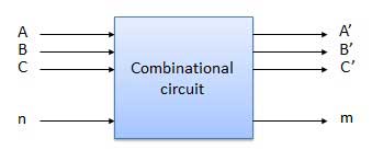
A combinational circuit can have an n number of inputs and m number of outputs.
BLACK DIAGRAM;
We're going to elaborate few important combinational circuits as follows.
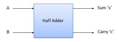
HALF ADDER;
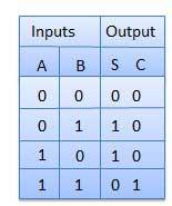
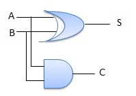
Half adder is a combinational logic circuit with two inputs and two outputs. The half adder circuit is designed to add two single bit binary number A and B. It is the basic building block for addition of two single bit numbers. This circuit has two outputs carry and sum.
BLOCK DIAGRAM;
TRUTH TABLE;
CIRCUIT DIAGRAM;
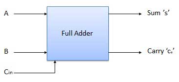
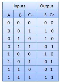
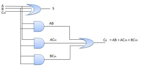
FULL ADDER;
Full adder is developed to overcome the drawback of Half Adder circuit. It can add two one-bit numbers A and B, and carry c. The full adder is a three input and two output combinational circuit.
BLACK DIAGRAM;
TRUTH TABLE;
CIRCUIT DIAGRAM;
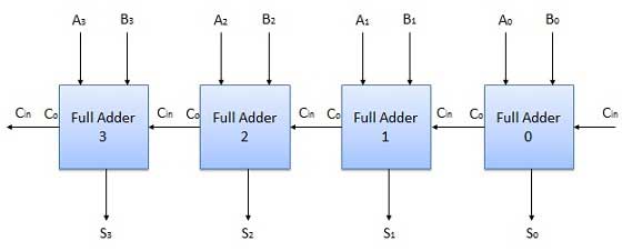
N-BIT PARALLEL ADDER;
The Full Adder is capable of adding only two single digit binary number along with a carry input. But in practical we need to add binary numbers which are much longer than just one bit. To add two n-bit binary numbers we need to use the n-bit parallel adder. It uses a number of full adders in cascade. The carry output of the previous full adder is connected to carry input of the next full adder.
4 BIT PARALLEL ADDER;
In the block diagram, A0 and B0 represent the LSB of the four bit words A and B. Hence Full Adder-0 is the lowest stage. Hence its Cin has been permanently made 0. The rest of the connections are exactly same as those of n-bit parallel adder is shown in fig. The four bit parallel adder is a very common logic circuit.
BLACK DIAGRAM;
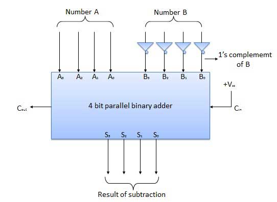
N-BIT PARALLEL SUBTRACTOR;
The subtraction can be carried out by taking the 1's or 2's complement of the number to be subtracted. For example we can perform the subtraction (A-B) by adding either 1's or 2's complement of B to A. That means we can use a binary adder to perform the binary subtraction.
4 BIT PARALLEL SUBTRACTOR;
The number to be subtracted (B) is first passed through inverters to obtain its 1's complement. The 4-bit adder then adds A and 2's complement of B to produce the subtraction. S3 S2 S1 S0 represents the result of binary subtraction (A-B) and carry output Cout represents the polarity of the result. If A > B then Cout = 0 and the result of binary form (A-B) then Cout = 1 and the result is in the 2's complement form.
BLACK DIAGRAM;
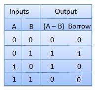
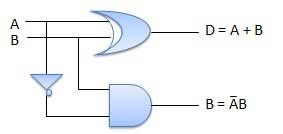
HALF SUBTRACTORS;
Half subtractor is a combination circuit with two inputs and two outputs (difference and borrow). It produces the difference between the two binary bits at the input and also produces an output (Borrow) to indicate if a 1 has been borrowed. In the subtraction (A-B), A is called as Minuend bit and B is called as Subtrahend bit.
TRUTH TABLE;
CIRCUIT DIAGRAM;
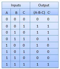
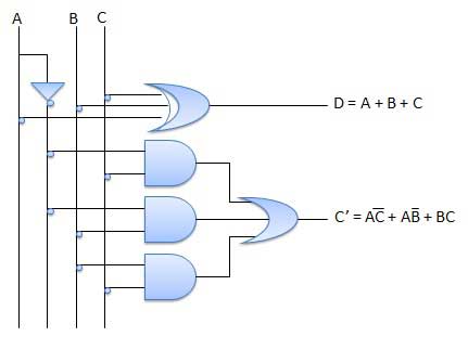
FULL SUBTRACTORS;
The disadvantage of a half subtractor is overcome by full subtractor. The full subtractor is a combinational circuit with three inputs A,B,C and two output D and C'. A is the 'minuend', B is 'subtrahend', C is the 'borrow' produced by the previous stage, D is the difference output and C' is the borrow output.
TRUTH TABLE;
CIRCUIT DIAGRAM;
MULTIPLEXERS;
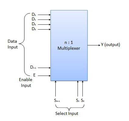
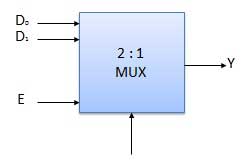
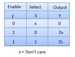
Multiplexer is a special type of combinational circuit. There are n-data inputs, one output and m select inputs with 2m = n. It is a digital circuit which selects one of the n data inputs and routes it to the output. The selection of one of the n inputs is done by the selected inputs. Depending on the digital code applied at the selected inputs, one out of n data sources is selected and transmitted to the single output Y. E is called the strobe or enable input which is useful for the cascading. It is generally an active low terminal that means it will perform the required operation when it is low.
BLACK DIAGRAM;
MULTIPLEXERS COME IN MULTIPLE VARIATIONS;
- 2 : 1 multiplexer
- 4 : 1 multiplexer
- 16 : 1 multiplexer
- 32 : 1 multiplexer
BLACK DIAGRAM;
TRUTH TABLE;
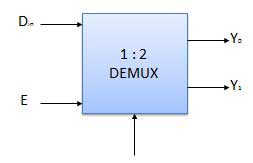
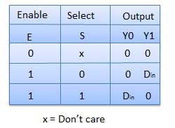
DEMULTIPLEXERS;
A demultiplexer performs the reverse operation of a multiplexer i.e. it receives one input and distributes it over several outputs. It has only one input, n outputs, m select input. At a time only one output line is selected by the select lines and the input is transmitted to the selected output line. A de-multiplexer is equivalent to a single pole multiple way switch as shown in fig.
DEMULTIPLEXERS COMES IN MULTIPLE VARIATIONS;
- 1 : 2 demultiplexer
- 1 : 4 demultiplexer
- 1 : 16 demultiplexer
- 1 : 32 demultiplexer
BLACK DIAGRAM;
TRUTH TABLE;
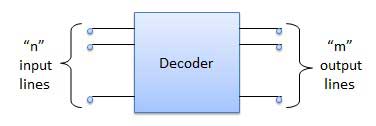
DECODER;
A decoder is a combinational circuit. It has n input and to a maximum m = 2n outputs. Decoder is identical to a demultiplexer without any data input. It performs operations which are exactly opposite to those of an encoder.
BLACK DIAGRAM;
EXAMPLES OF DECODERS ARE FOLLOWIMG;
- Code converters
- BCD to seven segment decoders
- Nixie tube decoders
- Relay actuator
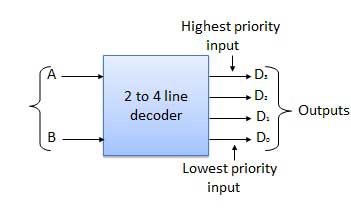
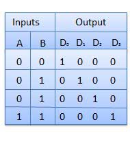
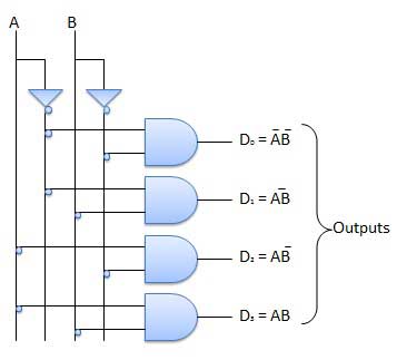
2 to 4 LINE DECODER;
The block diagram of 2 to 4 line decoder is shown in the fig. A and B are the two inputs where D through D are the four outputs. Truth table explains the operations of a decoder. It shows that each output is 1 for only a specific combination of inputs.
BLACK DIAGRAM;
TRUTH TABLE;
LOGIC CIRCUIT;
ENCODER;
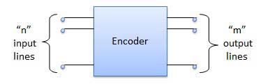
Encoder is a combinational circuit which is designed to perform the inverse operation of the decoder. An encoder has n number of input lines and m number of output lines. An encoder produces an m bit binary code corresponding to the digital input number. The encoder accepts an n input digital word and converts it into an m bit another digital word.
BLACK DIAGRAM;
EXAMPLES OF ENCODERS ARE FOLLOWING;
- Priority encoders
- Decimal to BCD encoder
- Octal to binary encoder
- Hexadecimal to binary encoder
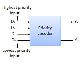
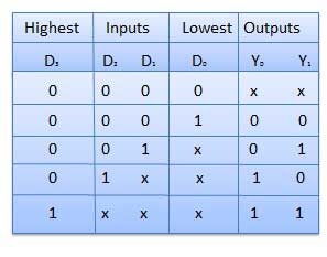
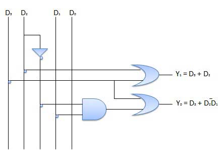
PRIORITY ENCODER;
This is a special type of encoder. Priority is given to the input lines. If two or more input line are 1 at the same time, then the input line with highest priority will be considered. There are four input D0, D1, D2, D3 and two output Y0, Y1. Out of the four input D3 has the highest priority and D0 has the lowest priority. That means if D3 = 1 then Y1 Y1 = 11 irrespective of the other inputs. Similarly if D3 = 0 and D2 = 1 then Y1 Y0 = 10 irrespective of the other inputs.
BLACK DIAGRAM;
TRUTH TABLE;
LOGIC DIAGRAM;
MORE DETAILS;
https://youtu.be/U5rcEkIJYiI
OR
Comments
Post a Comment